This page provides a few excerpts from a document in preparation tentatively called, "Inside the TIA". The purpose of the document is to present a detailed analysis of the Atari TIA (Television Interface Adapter) chip with schematic diagrams, circuit descriptions and timing charts. Reference documents supporting this work included copies of scans of an original set of TIA schematics done by Mark De Smet. A logic simulator, designed for use with TIA circuits, was used to produce all timing diagrams.
NOTE: These excerpts are only snippets of text and diagrams in preparation. They are not organized into any coherent form and are only posted here to provide a preliminary look at the contents of the document.
There are several timing signals generated in the TIA to synchronize critical operations of the game system. An external master oscillator, running at 3.58 MHz, defines the pixel interval and is subdivided by hardware to provide other signals for horizontal positioning and control. The system CPU, a 6507, is driven by a f0 (phase 0) clock, from which it generates the f1 and f2 clock signals required for read/write control.
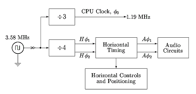
Top Level Clock Signals
In this block diagram, the relation between the on board master oscillator, 3.58 MHz, and some of the derived critical time signals is shown. These blocks will be examined in detail in the following paragraphs.
The first circuit to be examined is the circuit which develops the CPU clock. It consists of a pair of flip flops configured as a two-stage counter with feedback to reset on every third count, forming a divide by three. A schematic diagram is given below. (The diagram does not show an external Master Reset line, since it was not needed in the simulation.)
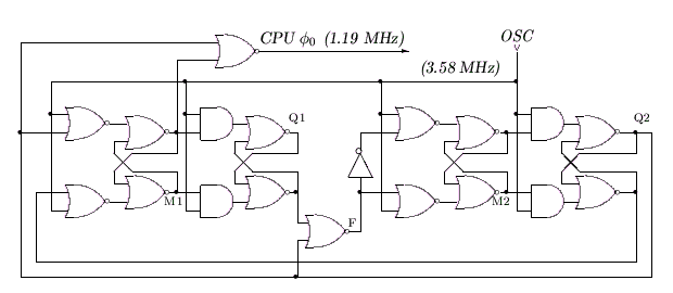
CPU Clock Generation (Divide by 3)
This circuit divides the master oscillator frequency by 3, producing a symmetrical square wave for the CPU. Critical nodes are labeled in the schematic diagram and the waveforms which appear there are shown in the chart below. This chart was produced from signal data generated by the simulator.
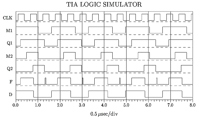
Timing Chart for Divide by 3
The time between major divisions is 0.5 msec, so the total displayed time period is 4.0 msec. Note the transient which appears at the output of the feedback control gate, F. It occurs when the clock goes high, but only persists for about 1 gate delay. Since the simulator operates with about 8 gate delays between changes of the clock, and 3 gate delays occur before gate D changes, there is a noticeable offset between the master clock, OSC, and the CPU clock, D. This offset is an artifact of the sampling frequency used in the simulation. The advantage of a low rate is that it makes the tracking of gate delays easier. A disadvantage is that signals which propagate over many delays may not be properly represented. The general rule is that the longest path must be shorter than the shortest clock interval. All simulations are carefully controlled to meet this requirement.
The horizontal scan counter provides decoders for several critical events. Each decoder produces a single pulse whose width is 4 pixel clocks (1.12 µsec). For example, the Horizontal Blank signal, HB, is started from SHB and terminated with RHB or LRHB, depending on whether an HMOVE has taken place. When LRHB terminates the HB signal, the blank interval extends into the first 8 pixels of the screen, as has been often discussed.
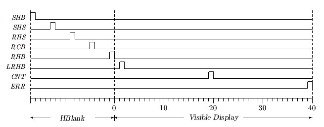
Decoded Critical Horizontal Events
The playfield generator consists of the data registers PF0, PF1 and PF2 and two 20-bit shift registers which run continuously. One of the registers shifts right and the other shifts left. In operation, a single '1' bit is shifted in at the start of the playfield and this bit cycles through the appropriate register, effectively selecting one playfield bit per clock. The PF GRAPHICS output presents the selected playfield bit to the graphics control system. The diagram below shows the conceptual organization of the circuits, but the peculiar reversal of the PF1 bits is explained elsewhere and not shown here.
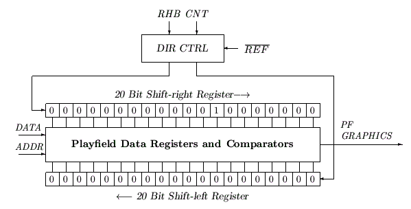
Playfield Registers and Controls
Note that the upper, shift-right, register will always receive a one bit from the Reset Horizontal Blank ( RHB) line and this will start the forward display of the first 20 bits of the playfield. In the above diagram, the active '1' bit is at the 13th playfield bit position. The Center (CNT) bit is routed to the shift-right register or the shift-left register depending on the state of the reflect bit (REF).
The playfield registers can be changed at any time (within CPU clocking limits) and the only other critical timing issue under user control involves the REF signal. Its effect on the playfield generator is in routing the single bit identified by CNT to one of the shift registers.Any changes in REF which occur before or after CNT is high have no effect -- only its value when the routing takes place.
With the TIA Simulator it is possible to ferret out the exact behavior of the TIA internal circuit blocks. One of the more interesting of these is the subsystem devoted to fine tuning the placement of objects by adding or subtracting clock pulses from the positioning circuits. The circuit which produces 'extra' clocks also has side effects which have been exploited in some games. Although the details of these side effects have been documented and confirmed by analysis and experimental testing, the simulator provides an additional resource for investigating boundary conditions and critical timing issues. Below are two screen shots of simulations of the extra clock circuits with changes to the Horizontal Motion register occurring at different times.
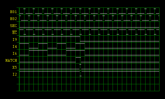
Screen Shot of TIA Simulator Exercising 'Extra Clock' Circuits
The display shows the state of the signal which resets the extra clock latch (labeled MATCH) and confirms that if this signal is cleared prior to the trailing edge of H01, extra clocks will continue to occur. For this run, the Horizontal Motion register is changed just before the critical time so that the latch misses its reset. Signal I9 is the high bit in the motion register and is switched from high to low just before the latch is set.
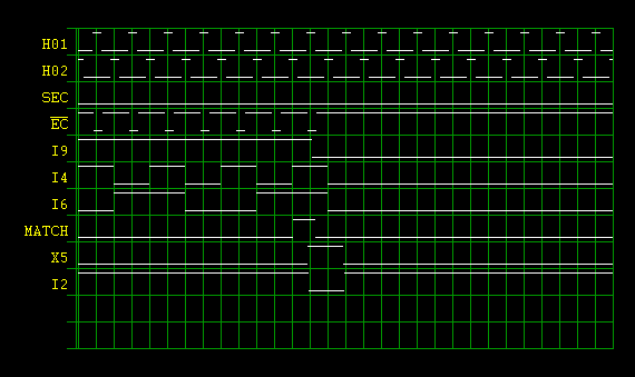
In this run, the change in I9 was delayed very slightly so that the MATCH condition was high during the trailing edge of H01. Hence, it was too late to stop the extra clock latch from resetting. This level of timing control is possible with the simulator, but to determine the actual limits faced by the programmer, it is necessary to synchronize the change in I9 to the CPU clock f2 and see which cycles are critical. This is easy to do with the simulator, but observe that the change in I9 may occur near the leading edge of the write to the Horizontal Motion register (about the middle of the last CPU cycle of the write instruction).
The audio output from the TIA is derived from a frequency divider and various configurations of two linear feedback shift registers. A 4-bit register and a 5-bit register account for the amazing flexibility of this subsystem. The 4-bit version, shown below, is responsible for several of the sound/noise options. A full description of this circuit, explaining its operation in all Audio Control modes is included in the document, but not reproduced here.
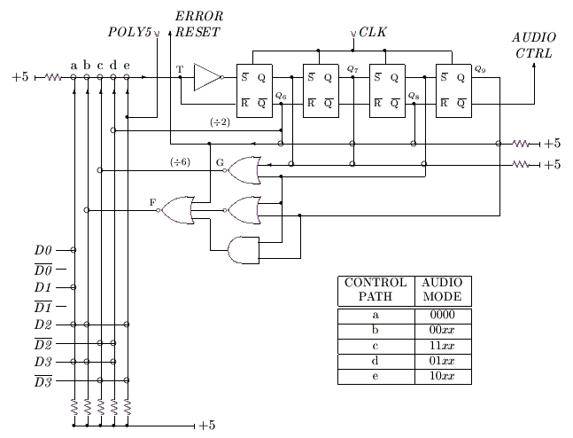
4-Bit Polynomial Shift Register and Controls