
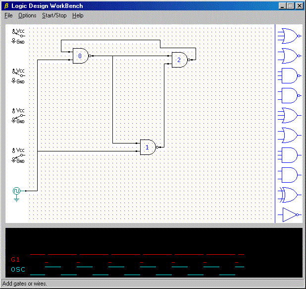
The Logic Design Workbench (LDW) is an amazingly simple and easy to use logic simulator intended for use by students and logic designers. It allows you to select basic logic elements for placement on the layout grid and to run wires between nodes with simple clicks of the mouse. A built in oscillator provides automatic square wave signals whenever a simulation is running, and on-screen switches provide a means for user interaction with the circuit. Three signal probes are available to monitor key circuit nodes. A full Windows Help system is provided as are a few loadable example files.
Have you ever wondered how complex logic blocks are constructed from simple gates? How can we derive the governing equations for a `D' flip-flop, or a clock separator, or an up-down counter controller? This monograph, Advanced Logic Design Techniques in Asynchronous Sequential Circuit Synthesis, provides a complete method for taking the design from its initial problem statement to the final, fully implemented circuit. The file is provided as an Acrobat (*.pdf) file and includes over 60 pages of design methodology and logic design examples. Full treatment is given for designing edge-triggered flip-flops, divide-by-two circuits, synchronous clock stream switches, digital single shots, pulse generators, etc. from simple gates.
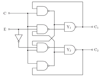
Synchronous Clock Stream Switch
The circuit example above, designed with the methods presented in the monograph, switches the input clock stream (C) to one of two output lines under control of the enable line (E). Note the use of the term synchronous, which here means that the outputs are synchronized with the clock line so that only full-length output clock signals are passed through, even though the enable line may be totally asynchronous with the clock.
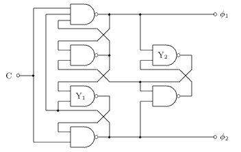
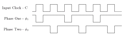
Two-phase Clock Generator
This is another example taken from the monograph. This circuit is sometimes referred to as an underlapped clock generator.
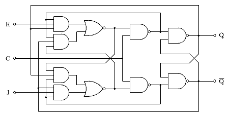
Edge-triggered J-K Flip-Flop
This flip-flop does not exhibit the anomalous ones-catching behavior characteristic of master/slave J-K flip-flops. A full treatment of the derivation of its design equations and their implementation is covered in the monograph.
Here is a logic design for a divide-by-three circuit with special phase requirements. This circuit is not covered in the monograph, but is described and implemented in a companion paper, Designing a Divide-by-Three Logic Circuit, available here. The methods used in this paper are, of course, based on those presented in the above monograph and the reader is assumed to be familiar with that document.
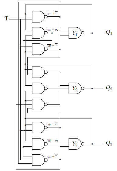
Divide-by-Three with Overlapped Phases
It is noted in the paper that few logic designers, when confronted with a need for a divide-by-three circuit, will immediately proceed with a gate level solution. More often, the designer will consider higher level logic blocks, such as flip-flops or shift registers and reduce the design problem to that of configuring the support logic. This is a perfectly legitimate approach. At times, however, the advantages of a gate level design are simply too many to ignore or the goal is to produce and integrated circuit. This is one such solution.
Here is a circuit which is similar to a 'D' flip-flop, except that it transfers the input data to the output on every clock edge, not just those of a single polarity.
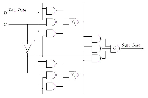
Data Synchronizer
A paper describing the design in detail is available here. Note that the operation of the circuit is such that it may find application in digital filters, correlators, phase detectors, noise suppressors, etc.
Synchronous counters, unlike ripple counters, have all stages clocked simultaneously. This eliminates spurious output combinations that occur in ripple counters as the count propagates from the lowest stage to the highest. To fabricate synchronous counters from 'D' flip-flops, it is only necessary to wire all clock inputs together and find appropriate gating functions for each 'D' input. The gating functions can be found by treating the counter as a simple state machine and generating a Karnaugh map whose cells represent current states and whose cell contents represent next states.
Suppose a 4-bit synchronous binary counter is required. Let the stages, from lowest to highest, be Q0, Q1, Q3 and Q3. Then the equation for Q3 will be
Q3+ = Q3*Q2*Q1*Q0 + Q3*(Q2+Q1+Q0),
where it is understood that the value on the left side is the next state and the values on the right are the current state. Also, the Boolean AND operator is denoted by the '*' character and the OR by the '+' character.
This equation can be put in a simpler form by first applying DeMorgan's theorem to the quantity in parentheses.
Q2+Q1+Q0 = Q2*Q1*Q0.
We now have
Q3+ = Q3*(Q2*Q1*Q0) + Q3*(Q2*Q1*Q0),
which we recognize as an EXCLUSIVE OR function. Using the '^' operator for the EXCLUSIVE OR, the last equation can be simplified to
Q3+ = Q3 ^ (Q2*Q1*Q0).
This equation is in a form that can be applied recursively to each stage in the synchronous counter. The 'D' input to each stage is simply the EXCLUSIVE OR if its own output with the product of all lower stage outputs. For Q0, the product of lower stages is taken as '1'. Recall, however, that simplifying a Boolean expression does not necessarily result in a simplified implementation.